Bias frames
The bias level represents an effective zero level which is present in all frames. This must be subtracted before any other stages of the data reduction process take place. Consquently, the bias level should ideally have long-term stability. For this camera the level is typically about 220 ADU in the active chip area, but varies slightly with location. The spatial dependency of the bias and its variation with temperature are analysed here. The read noise is derived from the bias frames and is assessed for the presence of any non-random components.
Bias frame structure
The camera was configured with the overscan region turned on. An single bias frame at -20C, with overscan, is shown below.

The active chip area comprises a region 2184 by 1472 pixels. The overscan region consists of two distinct areas: the area outlined in orange contains a further 37 pixels per row that are part of the chip structure but are not part of the imaging area, whilst the area outlined in magenta is obtained by clocking the read-out register for another 200 cycles per row, thereby giving the impression of an additional 200 pixels. These are artificial pixels and contain just read noise.
To assess the bias frames for the presence of any structure, a series of 100 bias frames was made and then combined using a broadened median. An average section in the 'X' direction was constructed by summing all the rows and dividing by their total number. This was repeated for a range of temperatures. These sections are shown in the plot below.

The bias level in the active chip area varies with column number and is dependent on temperature. The spikes arise from charge smearing from point defects on the chip as each row is clocked down past that point during the read-out process. These effects are drastically reduced at the lower temperatures. The amplifier bias, shown in the overscan region, has a constant level of about 200 ADU that does not vary significantly with temperature.
The following plot shows average 'Y'-sections taken through both the active chip area and the part of the overscan region containing just the read noise.
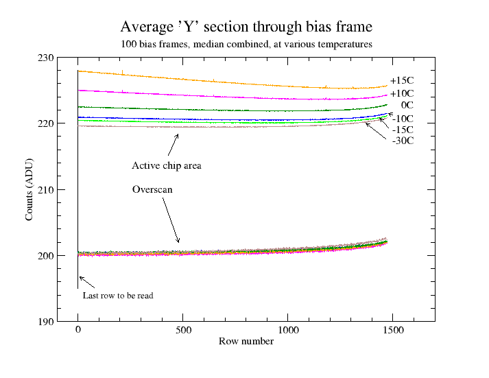
There is some variation in the bias slope with row number, although this decreases with decreasing temperature. Note that row zero represents the last row to be read. If the inherent variation with row number that is present in the overscan region is subtracted from the bias level in the active imaging region, the following graph is obtained:
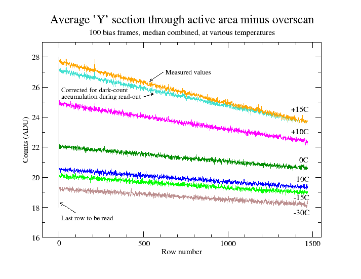
These curves show a simple linear dependency of bias level on row number and there is none of the more complex structure visible in the 'X'-section plots. The pale blue curve shows the expected true bias level variation at +15C after allowing for accumulation of dark counts during read-out of the image. It is calculated using the mean dark count rate in ADU at +15C (see Dark signal) and an assumed read-out time of 8s. This effect is not suffficient to account for the slope of the bias level completely, and neither does it explain the variation in overall bias level with temperature. This temperature dependency must be accepted as an inherent feature.
Bias frame stability
Bias frame structure is of little consequence if the bias level is stable and can be subtracted reliably. To test the bias frame stability, two master bias frames were constructed, each comprising 100 bias frames at -20C, combined using a broadened median. The second master bias frame was made 70 days after the first. The newer master bias was divided by the older and the average 'X' section was extracted. This is shown below.

The bias level in the active chip area of the new master bias frame is about 0.14% higher than in the old frame - equivalent to about 0.3 ADU, although with a slightly larger deviation at the edges. The amplifier bias in the part of the overscan region containing just read noise is about 0.03% lower in the new master bias frame, or about 0.06 ADU. Clearly the stability of bias frames is very good.
If bias frames were taken before any other exposures after turning the camera on and cooling down, it was noted that the first bias frame always had a mean level about 1 ADU higher than the others. This is presumably due to thermal charge: it could always be remedied by performing an aggressive flush of the CCD before the first frame. Alternatively, the first bias frame in such cases should be discarded.
Bias frame subtraction
The mean bias level varied by a maximum of about 1.5 ADU within any of the sets of 100 bias frames taken at various temperatures. Assuming that this variation is typical of CCD exposures in general, the largest systematic (i.e. non-random) error in bias subtraction is thus likely to be about +/- 0.75 ADU for subtraction of a master bias frame made of 100 bias exposures from a single CCD exposure.
It is sometimes suggested that the overscan region be used to estimate the bias offset for any given frame. However, it was found that the level in the 'read noise' part of the overscan region for a 'light' frame can be up to 20 or 30 ADU higher than the base level of 200 ADU; this is clearly seen for flat-field frames. Therefore no reliable estimate can be made from the overscan region and the best method of de-biasing is a straight subtraction of a master bias frame.
Read noise
The true read noise is obtained from the area of the overscan region that contains just the read noise. The bias level that is present in the active imaging area varies from pixel to pixel and thus contributes its own noise. This gives rise to an apparent read noise (higher than the true read noise) that will always be present in each frame in practice. Because the bias level varies over the surface of the chip, the apparent read noise does also, being slightly higher at the edges than in the middle. This effect is very small.
The true and apparent read noise were measured at a range of temperatures. For each measurement at any given temperature, each set of 100 bias frames was divided into 50 pairs, and the second of each pair was subtracted from the first. Taking the difference of two bias frames removes any fixed pattern noise that may be present and enables a good estimate of just the read noise to be made. The standard deviation of each difference frame was measured in the centre of the active area for the apparent read noise, and in the centre of the 'read noise' area of the overscan region for the true read noise. A square 100 pixels on a side was used in both cases. The standard deviation was then divided by the square root of two (subtracting one frame from the other doubles the variance of the data). An average of all fifty such measurements at any temperature was then calculated. Furthermore, because each read noise estimate comprised fifty measurements, an estimate of the error in the read noise could also be made. The values, with their error bars, are plotted below.

The true and apparent read noise values are tabulated below, using a gain of 1.33 e/ADU.
| Temperature (Celsius) | True (ADU) | Apparent (ADU) | True (electrons) | Apparent (electrons) |
|---|---|---|---|---|
| +15 | 6.85+/-0.05 | 8.33+/-0.06 | 9.11+/-0.06 | 11.08+/-0.07 |
| +10 | 6.69+/-0.04 | 8.10+/-0.06 | 8.89+/-0.06 | 10.77+/-0.09 |
| +5 | 6.61+/-0.05 | 7.99+/-0.06 | 8.80+/-0.06 | 10.62+/-0.08 |
| 0 | 6.61+/-0.04 | 7.91+/-0.07 | 8.79+/-0.06 | 10.52+/-0.09 |
| -5 | 6.62+/-0.04 | 7.90+/-0.08 | 8.80+/-0.06 | 10.51+/-0.11 |
| -10 | 6.68+/-0.04 | 7.87+/-0.06 | 8.88+/-0.06 | 10.47+/-0.08 |
| -15 | 6.73+/-0.05 | 7.87+/-0.06 | 8.96+/-0.06 | 10.47+/-0.08 |
| -20 | 6.76+/-0.05 | 7.85+/-0.06 | 8.99+/-0.06 | 10.45+/-0.08 |
| -25 | 6.86+/-0.05 | 7.94+/-0.07 | 9.12+/-0.07 | 10.56+/-0.09 |
| -30 | 6.84+/-0.05 | 7.90+/-0.08 | 9.09+/-0.07 | 10.50+/-0.11 |
Assessment of read noise for non-random components
Ideally, any CCD exposure should consist of nothing more than the signal from the target object. In practice, all CCD exposures include bias level, dark signal, and read noise. If these additional components have purely random noise (with a gaussian distribution) then the noise component can (in principle) be made arbitrarily small by stacking sufficient exposures and using appropriate methods for bias and dark signal subtraction. Any additional non-random sources of noise from e.g. electronic interference can be seen as additional components to the read noise. Such non-random effects will tend to add rather than averaging out when exposures are added, thus preventing the detection of faint sources and making accurate analysis of data frames more difficult.
To assess the nature of the read noise, a read noise frame was constructed by subtracting the average of thirteen individually selected bias frames (with no 'cosmic ray' events) from a single frame that was not used to form the average. This process removes the fixed pattern of the bias level. A central square area, 1024 pixels on a side, was extracted and the histogram of the noise is plotted below left, with a logarithmic y-axis. The histogram shows the symmetrical inverted parabolic shape of a log-gaussian distribution with no obvious additional non-random noise in the wings of the distribution.
A Fourier transform was taken of the 1024-pixel square area and the central 300 x 300 pixels of the power spectrum image is shown below right. The Fourier transform is very sensitive to non-random noise patterns in the original noise frame that may not be evident by eye. Such patterns may manifest themselves as stripes or other obvious shapes on the Fourier transform; however it appears to be free of any major defects.

